Bottom line: Nvidia took the wraps off its Hopper architecture at GTC 2022, announcing the H100 server accelerator but only showing off renders of it. Now we finally have some in-hand photos of the SXM variant of the card, which features a mind-boggling 700W TDP.
It's been a bit over a month since Nvidia unveiled their H100 server accelerator based on the Hopper architecture, and so far, we've only seen renders of it. That changes today, as ServeTheHome has just shared pictures of the card in its SXM5 form factor.
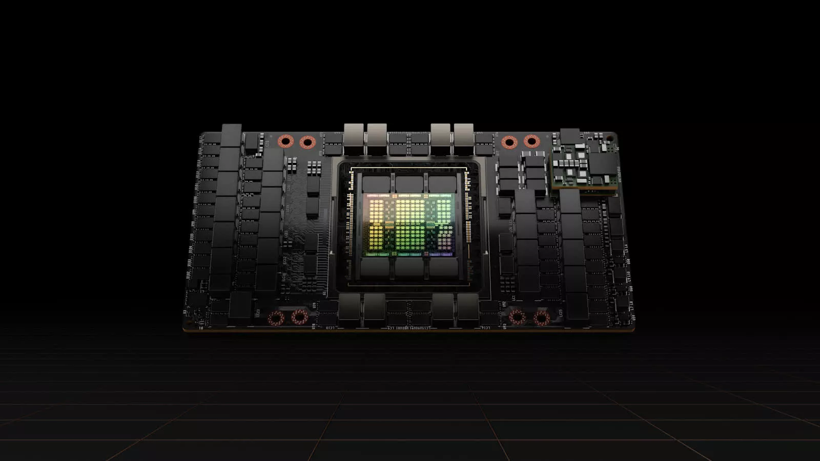
The GH100 compute GPU is fabricated on TSMC's N4 process node and has an 814 mm2 die size. The SXM variant features 16896 FP32 CUDA cores, 528 Tensor cores, and 80GB of HBM3 memory connected using a 5120-bit bus. As can be seen in the images, there are six 16GB stacks of memory around the GPU, but one of these is disabled.

Nvidia also quoted a staggering 700W TDP, 75% higher than its predecessor, so it's no surprise that the card comes with an extremely-impressive VRM solution. It features 29 inductors, each equipped with two power stages and an additional three inductors with one power stage. Cooling all of these tightly packed components will probably be a challenge.
Another noticeable change is the connector layout for SXM5. There's now a short and a long mezzanine connector, whereas previous generations featured two identically sized longer ones.

Nvidia will start shipping H100-equipped systems in Q3 of this year. It's worth mentioning that the PCIe version of the H100 is currently listed in Japan for 4,745,950 yen ($36,300) after taxes and shipping, although it has fewer CUDA cores, downgraded HBM2e memory, and half the TDP of the SXM variant.