
TL;DR: Google and the US government want to speed up design and manufacturing of new semiconductor devices, adopting the open source model to let universities and startups run wild with innovative ideas. The cooperative research and development agreement will allow the National Institute of Standards and Technology (NIST) to design, develop and produce open source chips that researchers and companies will be free to use and adapt in their applications.
A new agreement between the US Department of Commerce and Google could spark a surge of new chip designs and innovations. According to the DoC, the Google-NIST partnership answers one of the most pressing issues in the semiconductor industry: big corporations have ready access to new chips and designs, while universities, researchers and small businesses face a major hurdle as they try to create something new. An open source chip design, which can be used without restrictions or licensing fees, should accelerate innovation and bring costs down dramatically.
The agreement states that NIST, together with its many research partners (University of Michigan, University of Maryland, George Washington University, Brown University, Carnegie Mellon, and others), will provide new chip designs to be manufactured by Skywater Technology in Minnesota. Google will fund the initial manufacturing cost, subsidizing the first production run as well.
Also read: Hard vs. Soft: Software may be eating the world, but hardware monetizes better
The US government aim is to create a new and affordable domestic supply of chips for research and development, a way to "unleash the innovative potential" of researchers and startups.
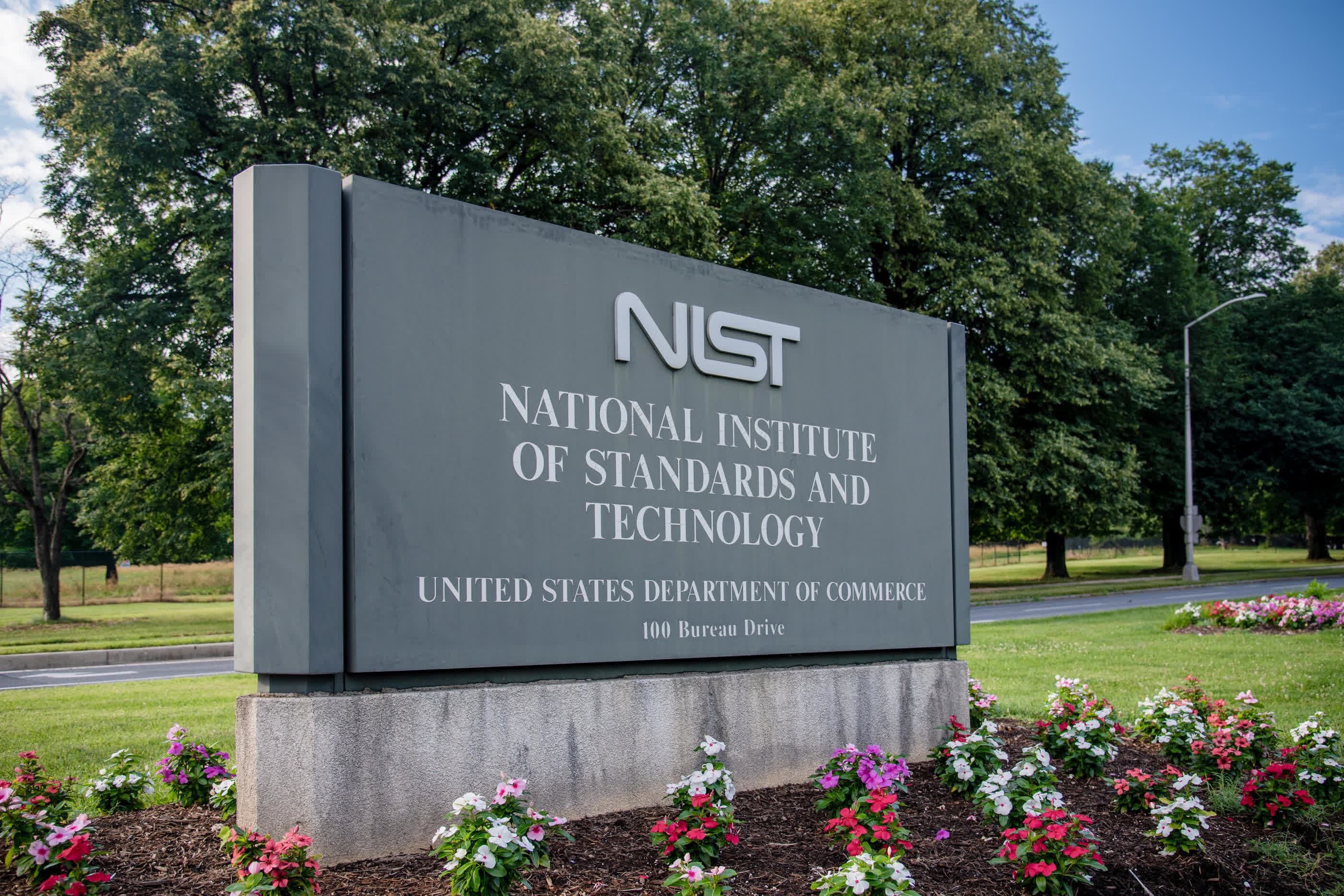
According to NIST director Laurie E. Locascio, the collaboration was planned before the introduction of the new CHIPS Act legislation, and it's an example of how government, industry, and academic can work together for the common goal of preserving the US leadership in the technology industry.
In NIST plans, almost 40 unique chip designs will be funded in partnership with Google to power different applications like new memory devices, nanosensors, bioelectronics, and chips for artificial intelligence and quantum computing. The open source designs will let researchers run wild with new ideas and share data without restrictions.
In presenting the new initiative, Google Public Sector CEO Will Grannis highlights the "long history of leadership in open source" of the Mountain View company. Public and private institutions will be able to iterate on each other's work, thus democratizing innovation in nanotechnology and semiconductor research. Chips will be produced in the Skywater foundry using industry-standard 200nm wafer discs, which universities and other partners will then dice into thousands of individual chips at their own processing facilities.